Summary:
Researchers at the University of Illinois Urbana-Champaign have developed a solid-state nanopore sensor using 2D materials, marking a major breakthrough toward ultra-fast, affordable, label-free DNA sequencing for precision medicine.
Takeaways:
- The team overcame long-standing fabrication challenges by using 2D materials like molybdenum disulfide and tungsten diselenide to build nanoscale diode-embedded nanopores.
- Their design enables simultaneous control and measurement of DNA translocation, a key step toward real-time, base-by-base sequencing.
- Future iterations aim to improve resolution and scalability, potentially enabling sequencing in under an hour at a fraction of today’s cost.
A pioneering partnership between researchers from The Grainger College of Engineering at the University of Illinois Urbana-Champaign has produced a novel nanopore sensing platform for single-biomolecule detection. Their findings, published in PNAS, pave the way for solid-state, label-free DNA sequencing technologies with implications for precision medicine.
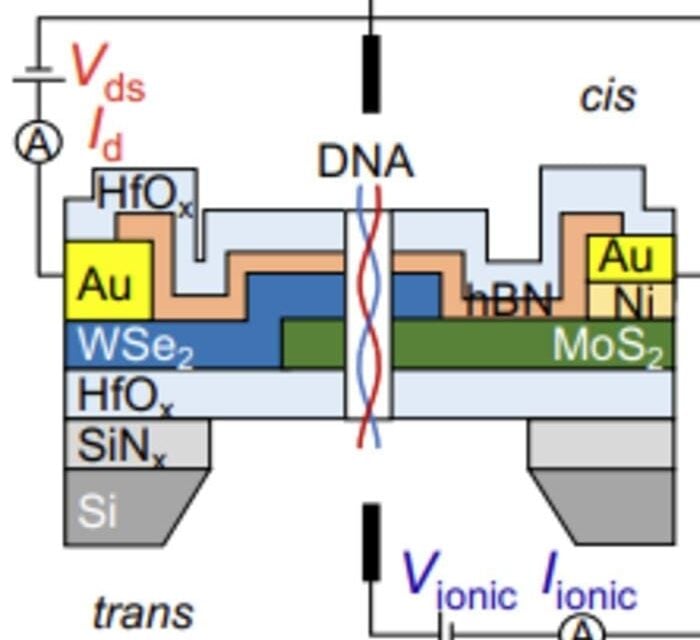
Nanopore sensors are tiny devices used to detect and analyze individual molecules by measuring ionic changes as the molecules pass through nanometer-scale openings. These sensors are classified into two types: one relying on biological materials, and the other on inorganic solid-state materials. DNA sequencing using biological nanopores is now commercially available, but Illinois Grainger engineers wanted to realize this technology using solid-state materials.
“Solid-state nanopores are compatible with wafer-scale manufacturing processes and therefore offer a significant advantage over biological nanopores for massively parallelized, low-cost sequencing,” said Sihan Chen, an Illinois Grainger postdoctoral researcher and the lead author of the paper.
Obstacles Towards Realizing Nanopore Sequencing
The major obstacle towards realizing solid-state nanopore sequencing is creating a sensor small enough to achieve base-by-base resolution as single molecules pass through the pore and to electrically read out the translocation of the molecules. In the late 2000s, IBM proposed the idea of DNA transistors, conceptualized with a dielectric metal sandwich structure and electrostatic traps to simultaneously allow ratchet-like control and sensing of DNA translocation. However, this structure was never realized experimentally because of the significant challenges involved in fabricating ultra-thin metal films encapsulated by dielectric layers using 3D materials.
“There had been a pause on the idea of solid-state DNA transistors for a decade or so until we revisited this idea using 2D materials,” Chen says.
Serendipitously, a collaboration was born between Arend van der Zande, a professor of mechanical science and engineering and materials science and engineering, and Rashid Bashir, a professor of bioengineering, Dean of The Grainger College of Engineering, and an affiliate faculty researcher in the Holonyak Micro & Nanotechnology Lab and the department of materials science and engineering. Both are also members of the Materials Research Lab. Bashir, an expert in the field of nanopore sensors, and van der Zande, an expert in the field of 2D materials, believed that combining their areas of interest to propose a new type of nanopore sensor could be timely and important.
The newly assembled research alliance began by identifying barriers to the realization of 3D biosensors. Ultra-thin 3D materials have rough surfaces—some with dangling bonds that inhibit electrical performance and limit the sensitivity to molecule translocation. The researchers realized that these limitations could be overcome by using 2D materials such as molybdenum disulfide and tungsten diselenide which naturally exist as monolayers with no dangling bonds.
“My lab specializes in stacking these monolayers on top of each other to engineer nearly any electronic device at sub-nanometer sizes” van der Zande says.
Measuring Changes in Electrical Current
The researchers integrated a 2D heterostructure into the nanopore membrane to create a nanometer-thick out-of-plane diode through which the molecule passes. This innovative design allowed them to simultaneously measure the changes in electrical current through the diode during DNA translocation and apply out-of-plane biases across the diode to control the speed of DNA translocation.
“We have used these new materials to finally realize a decades-old dream of the nanopore community that was previously impossible,” van der Zande says. “This work represents an important step towards base-by-base molecular control and opens doors to more advanced DNA sequencing technologies.”
Although the novel sensing platform has taken years to realize, it is expected to pay dividends in future precision medicine. Collecting genomic data from billions of patients to create tailored medicine and therapy regimens will require fast, reliable and affordable sequencing techniques, such as those demonstrated by the elite Illinois Grainger engineering team.
“In the future, we envision arrays of millions of 2D diodes with nanopores inside that could read out the sequences of DNA in parallel, reducing sequencing time from two weeks to as little as one hour,” Bashir says. Additionally, the researchers’ techniques could reduce the price of sequencing tenfold compared to current methods.
Next Generation Study Anticipated
Going forward, the researchers anticipate a next generation study utilizing alternating stacks of p-type and n-type 2D monolayers to improve upon the current iteration’s single p-n junction, which limits the quality of control over DNA translocation. A three-layer structure sandwiching an n-type layer between p-type layers will enable opposing electric fields to stretch the DNA, achieving the critical milestone of base-by-base DNA translocation control.
Until then, the powerhouse team of Illinois Grainger researchers will enjoy the fruits of their labor.
“We are at the frontier of 2D electronics, which we are bridging with the frontier of 3D nanopore sensing,” Bashir said. “We’re at two frontiers, and this intersection makes our project uniquely challenging and incredibly rewarding.”
Featured Image: Device architecture and measurement setup of an HJD-NP, with n-type MoS2 and p-type WSe2. Image: The Grainger College of Engineering at the University of Illinois Urbana-Champaign


